Section 5
Theory of Operation
DETAILED ANALYSIS
1. 11 MHz REFERENCE
OSCILLATOR
This oscillator runs at 11.1125 MHz on the AM mode and the frequency is
offset slightly higher or lower for USB or LSB respectively. The frequency
of this oscillator is also shifted slightly on receive by the clarifier
circuitry. TR-23 and L18 triple this oscillator giving a resultant frequency
of 33.335 MHz for one of the down mixer inputs. The second input will
come from the VCO.
2. VCO
The VCO will run at the operating frequency plus the local oscillator
frequency (7.800 MHz). This puts the VCO between 33.755 MHz at an operating
frequency of 25.995 MHz, and 35.800 MHz at an operating frequency of 28.000
MHz. The frequency of the VCO is controlled by a DC voltage varying between
0 and 5V coming from Coax #2. The higher the voltage, the higher the operating
frequency.
NOTE: A Varactor diode is the key to the VCO. This type of a diode changes capacitance as reverse bias is changed. The greater the reverse bias, the less capacitance and, therefore, the higher the frequency of the VCO. This diode is inside the VCO chip.
3. DOWN MIXER
TR-19 acts as the down mixer and mixes the VCO frequency with the 33 MHz
reference. The difference in the frequency of the two inputs will be the
down mixer output signal (460-2456 KHz). As an example, at a frequency
of 27.155 MHz (Ch. 16), the VCO frequency will be 34.955 MHz. The down
mixer will mix this frequency with the 33.335 MHz reference giving a difference
of 1.620 MHz for Channel 16 (See Fig. 34). This signal will be present
on TP10 and is used to drive the DS-400.
4. INPUT AMPLIFIER
The input amplifier inside the DS-400 is driven by the down mixer via
Coax #1. Diodes D5 and D6 protect the transistor Q1 from voltage spikes
which would otherwise open the base emitter junction to Q1. The diodes
also tend to square the signal waveshape. Q1 then amplifies the down mixer
signal to the necessary level to drive U15, the PLL synthesizer chip.
U15 requires 3V peak to peak minimum to drixe its input. This signal is
present on TP3 inside the 400 (See Figs. 21 & 31).
5. PROGRAMMABLE
DIVIDER (DIVIDE BY N)
The programmable divider divides the down mixer signal by a preset number.
The divider can divide by 2 through 512 depending upon the logic states
(0 or 5V) on its input pins 9-17. For proper operation the programmable
divider must have a 5 KHz output, the same as the fixed frequency divider.
For Channel 16 the input frequency must be 1.620 MHz. Therefore, the programmable
divider must divide by 324 to give a 5 KHz output. Frequency selection
is accomplished by changing the logic states on the input pins. Pin 17
is the least significant input and will change the VCO frequency by 5
KHz. Pin 9, the most significant pin, will change the frequency by 1280
KHz.
6. COUNTERS
The 40193 counters in the 400 drive pins 9-17 of the programmable divider.
Figure 34 gives some examples of what is happening in various parts of
the synthesizer for various frequencies. The 40193 binary counters add
or subtract from the programmable divider input when the DS-400 is stepped
up or down.
7. PROGRAMMING
SWITCHES
The programming switches preset the 40193 counters, such that radio will
be on 27.155 when the power is first applied. In other words, they control
the starting points for the counters. The display automatically starts
at 27.155 each time power is applied. Programming switches synchronize
the radio starting frequency with the DS-400 starting frequency.
8. PLL REFERENCE
FREQUENCY AND DIVIDER
Crystal X1 oscillates at 10.240 MHz using the oscillator in U15. This
signal is divided by 2 which gives an output of 5.1200 MHz on TP1 (See
Fig. 31). The fixed frequency divider then divides its input frequency
of 5.120 MHz by 1024. This results in a 5 KHz output which is used for
the channel spacing reference.
9. PHASE DETECTOR
The phase detector is considered the heart of the PLL and is the most
difficult to understand. Keep in mind for a proper "locked"
condition, both phase detector inputs must be the same frequency. The
reference input is always 5 KHz whereas the variable input could change
frequency if the VCO frequency were to change.
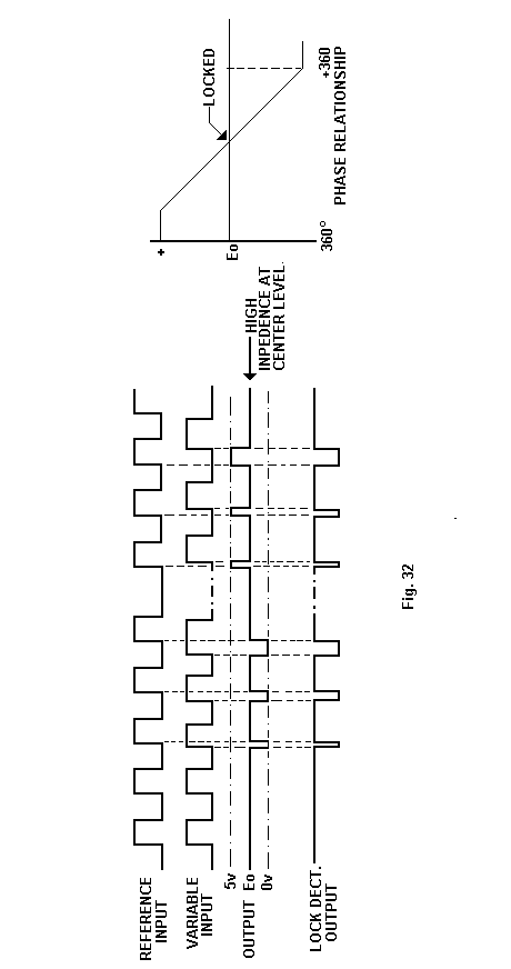
The detector uses a combination of digital logic gates which compare the phase of the variable input to the phase of the reference input. The phase detector looks at the rising edge of both its inputs simultaneously. As shown in Figure 32, if the phase of the reference and variable inputs are the same, the output will be at a mid-state or high impedence level. The reason for this will be explained in charge pump operation. If the frequency of the variable input should increase (variable lagging phase), the output (Eo) will go to a low (0V) state. Should the frequency of the variable input decrease causing the variable input to be leading phase, the output Eo will go to a high (5V) level.
9.1 LOCK DETECTOR
Figure 32 also illustrates the operation of the lock detector. If the
PLL is in lock, TP2 will be high (5V). If the PLL is out of lock, TP2
will be a low (OV) level. TP2 also drives the out of lock indicator circuitry
which will change the first digit on the DS-400 to an L when the PLL is
out of lock.

9.2 CHARGE PUMP
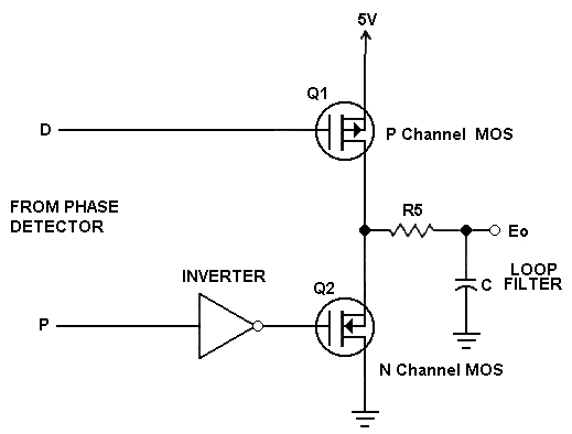
The schematic of the charge pump is shown below. The charge pump is considered
part of the phase detector.

Fig. 33 - Charge Pump
A CMOS IC is used
for the charge pump. As shown in Figure 33, this circuit is a pushpull
circuit with an inverter connected to one input. When D is 1 and P is
0, a positive voltage is applied to Q2 (N channel) by the inverter. Q2
is turned on and C discharges. When D is 0 and P is 1, Q1 (P channel)
is turned on and C is charged. When both D and P are 1, both Q1 and Q2
are turned off, Eo is floating and the voltage of C is held at the previous
value.
The hold time is inversly proportional to the gate leakage current of
Q1 and Q2. However, when the hold time becomes longer, Eo is maintained
at a fixed value and the VCO controlled by Eo is maintained at a constant
frequency for an extended period of time.
|
Operating
Frequency |
VCO
Frequency |
Down
Mixer
Output |
Programmable
Divider / By |
LOGIC
STATES AT PROGRAMMABLE DIVIDER
|
||||||||
|
17
|
16
|
15
|
14
|
13
|
12
|
11
|
10
|
9
|
||||
| 25.995 | 33.795 |
.46
|
92
|
0
|
0
|
1
|
1
|
1
|
0
|
1
|
0
|
0
|
| 26.500 | 34.300 |
.965
|
193
|
1
|
0
|
0
|
0
|
0
|
0
|
1
|
1
|
0
|
| 27.000 | 34.800 |
1.465
|
293
|
1
|
0
|
1
|
0
|
0
|
1
|
0
|
0
|
1
|
| 27.150 | 34.950 |
1.615
|
323
|
1
|
1
|
0
|
0
|
0
|
0
|
1
|
0
|
1
|
| 27.155 | 34.955 |
1.62
|
324
|
0
|
0
|
1
|
0
|
0
|
0
|
1
|
0
|
1
|
| 27.160 | 34.960 |
1.625
|
325
|
1
|
0
|
1
|
0
|
0
|
0
|
1
|
0
|
1
|
| 27.500 | 35.300 |
1.965
|
393
|
1
|
0
|
0
|
1
|
0
|
0
|
0
|
1
|
1
|
| 28.000 | 35.800 |
2.465
|
493
|
1
|
0
|
1
|
1
|
0
|
1
|
1
|
1
|
1
|
This
chart is correct for Uniden 8719 0
Represents Ov 1 Represents 5v
chassis with 11.1125 crystal only.
Figure 34
SUMMARY
Considering overall PILL operation, if the frequency of the VCO is assumed
to be higher than desired:
1. The down mixer
output frequency will be higher than desired.
2. The programmable divider output frequency will be above 5 KHz.
3. The phase detector will sense the variable input leading phase and
send out negative going pulses.
4. These pulses are filtered by the loop filter.
5. The decreased reverse bias is applied to the varactor diode on pin
5 of the VCO chip.
6. Because the capacitance of the varacotor diode controls the oscillating
frequency of the VCO, the VCO frequency will decrease and become locked
at the objective frequency.